French


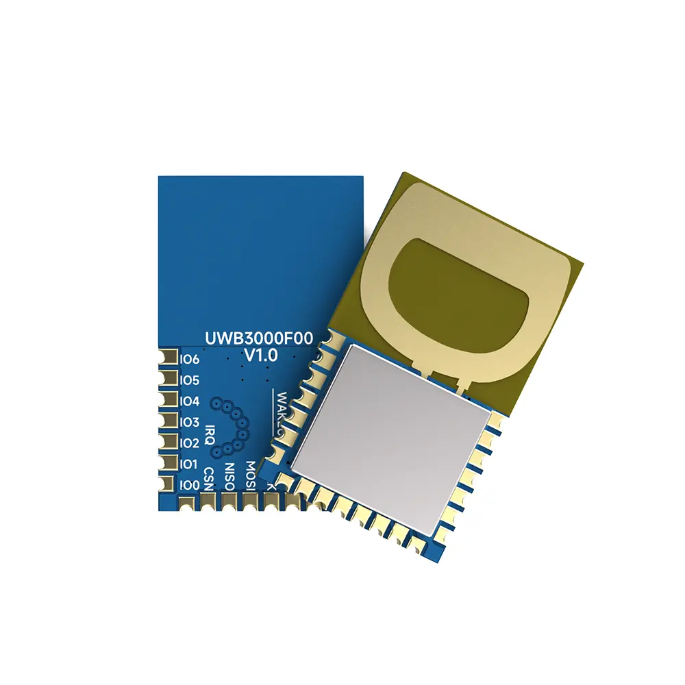
UWB3000F00 : Low-Power Bi-Directional Ranging Transceiver For Precision Positioning And Ranging
Output Power : 1mW
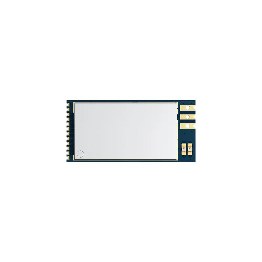
Size:13.5*22.2
Parameter | Condition | Min. | Typ. | Max. | Unit |
Supply Voltage | 3.0 | 4.2 | 5.5 | V | |
Operating Temperature Range | -20 | 25 | 60 | ℃ | |
Frequency Range | CH5 | 6489.6 | MHz | ||
RF Data Rate | 850k | 6.8M | bps | ||
Current Consumption | |||||
Sleep current | <100 | uA | |||
Transmit current 1 | Continues Frame mode | <350 | mA | ||
Receive current | 107 | mA | |||
Listen receive current | Low-Power SNIFF mode | <72 | mA | ||
Standby current | Receive off and no data transmission | 32 | mA | ||
RF parameter | |||||
Tx Power | @VCC=5.0V | -5 | 27 | dBm | |
Tx Bandwidth(BW) | 499.2 | MHz | |||
Receive parameters | |||||
Rx Sensitivity | @850Kbps | -100 | dBm | ||
@6.8Mbps | -94 | dBm | |||
Comply with IEEE 802.15.4-2020 Standard UWB and communication protocol
Supports UWB Channel 5 (6489.6 MHz)
Supports 6.8 Mbps and 850 Kbps RF Rate
Supports data frame lengths from 0 to 1023 bytes
Mesh networking
Multiple-level transmit power adjustment, with a maximum transmit power of 0.5W
1 km ultra-long-distance data communication
Supports two-way ranging methods SS-TWR and DS-TWR, as well as positioning solutions
Ranging accuracy less than ±10 cm
Supports multi-tag positioning with precise location calculation
Electrostatic Protection (ESD)
Personnel positioning in large-scale industrial production
Various indoor positioning scenarios
Underground coal mine positioning
Hospital staff positioning

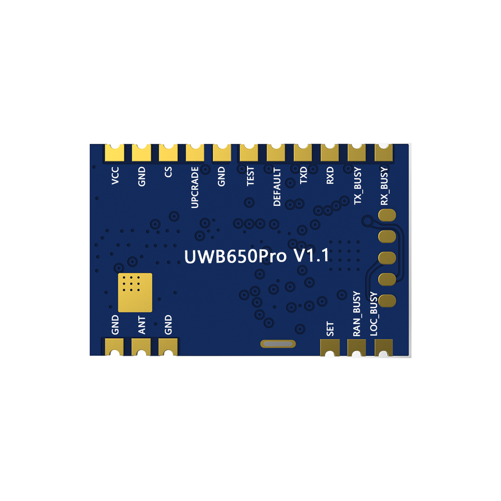
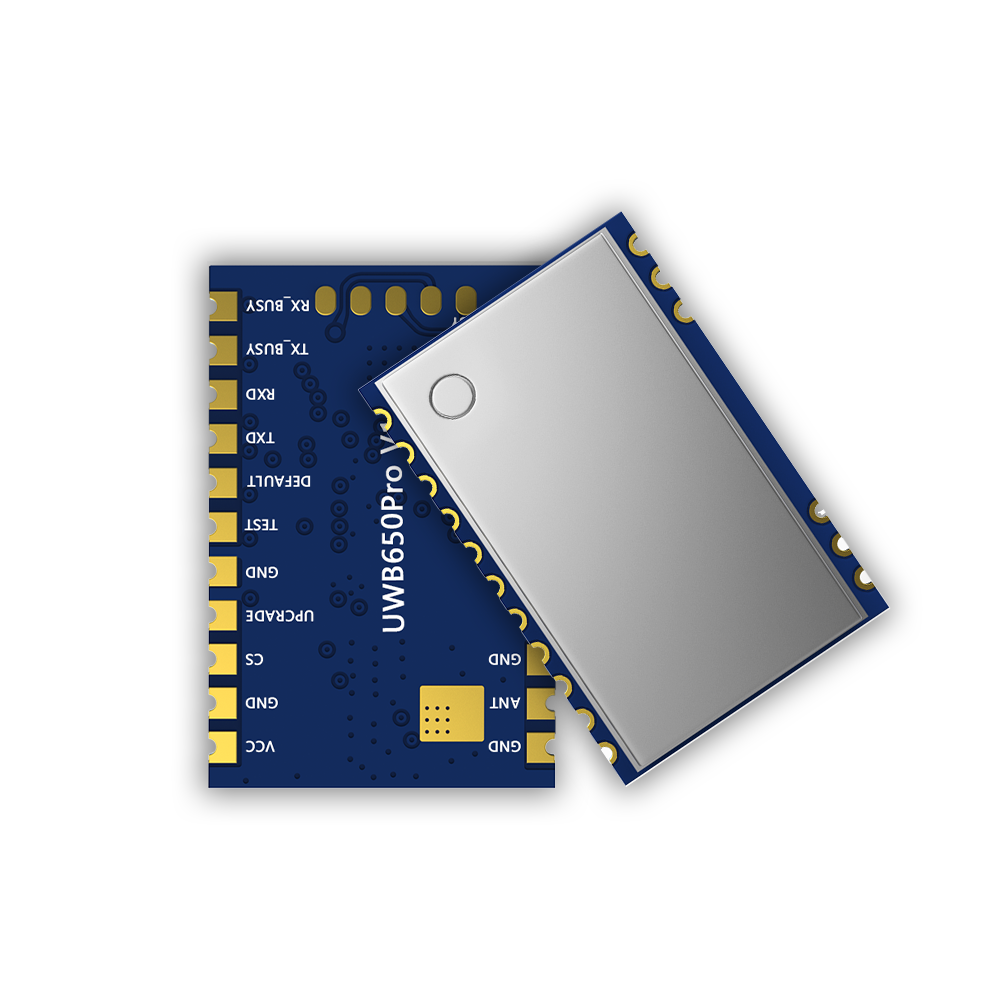
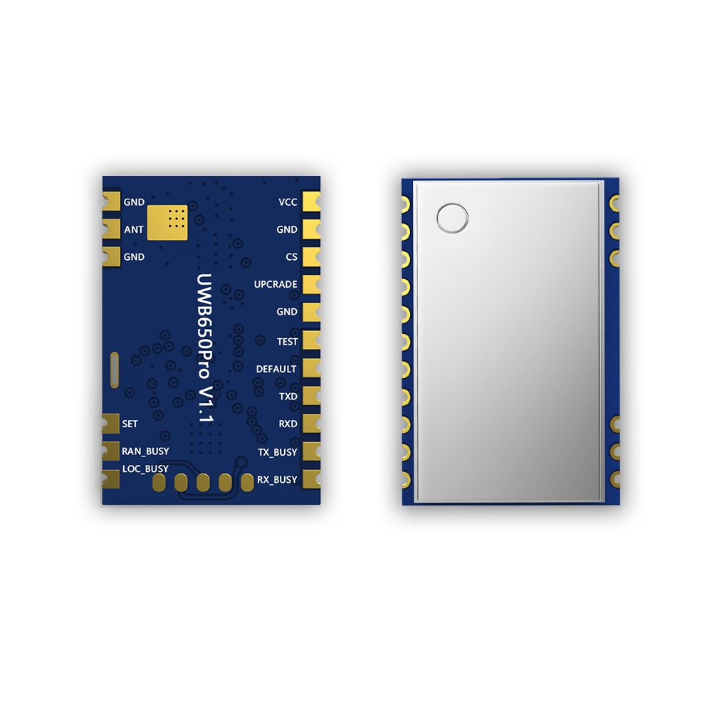
 side with numbered pins 1-17. The right image displays the bottom (PCB) side, labeling each pin, such as VCC, GND, TXD, RXD, and ANT.")
Pin No. | Pin definition | I/O | Voltage | Description |
1 | VCC | - | 3.0-5.5V | |
2,5,15,17 | GND | 0-3.3V | Connect to the power supply ground | |
3 | CS | I | 0-3.3V | Sleep pin, internally pulled up; the module enters sleep mode when a low level is applied externally |
4 | UPGRADE | I | 0-3.3V | Internally pulled up; after an external low-level input, the module resets and enters serial upgrade mode |
6 | TEST | I | 0-3.3V | - |
7 | DEFAULT | I | 0-3.3V | Internal pull-up, hold low for about 10s during operation to force a reboot and restore factory settings. |
8 | TXD | O | 0-3.3V | Serial data output pin, connected to the RXD pin of the external device |
9 | RXD | I | 0-3.3V | Serial data input pin, connected to the TXD pin of the external device |
10 | TX_BUSY | O | 0-3.3V | Transmit status indicator pin. Outputs HIGH during data transmission and returns LOW when transmission is complete.. |
11 | RX_BUSY | O | 0-3.3V | Receive status indicator pin. Outputs HIGH when data is being received and returns LOW when reception is complete. |
12 | LOC_BUSY | O | 0-3.3V | Positioning status indicator pin. Outputs HIGH when the module is performing positioning with other modules; outputs LOW otherwise. |
13 | RAN_BUSY | O | 0-3.3V | Ranging status indicator pin. Outputs HIGH when the module is performing ranging with other modules; outputs LOW otherwise. |
14 | SET | I | 0-3.3V | Module mode control pin, internally pulled up. When HIGH, the module operates in normal mode, allowing standard data transmission and command execution. |
16 | ANT | External 50 Ω antenna |
 by 20.00 ± 0.5mm (width) by 3.10 ± 0.1mm (height).")
Privacy Policy
· Privacy Policy
There is currently no content available
Email:sales@nicerf.com
Tel:+86-755-23080616